Share


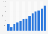
The global Conductor Etch System market size was valued at approximately USD 5.5 billion in 2025 and is projected to reach USD 10.7 billion by 2035, growing at a CAGR of 6.9% during the forecast period. Conductor etch systems play a critical role in semiconductor manufacturing, enabling the precise patterning required for device miniaturization and complex integrated circuits. These systems are integral to the process of transferring a pattern from a mask to a substrate by selectively removing material. The market comprises a range of etching technologies and solutions utilized by semiconductor manufacturers to optimize chip performance and production efficiency.
The global Conductor Etch System market size was valued at approximately USD 5.5 billion in 2025 and is projected to reach USD 10.7 billion by 2035, growing at a CAGR of 6.9% during the forecast period. Conductor etch systems play a critical role in semiconductor manufacturing, enabling the precise patterning required for device miniaturization and complex integrated circuits. These systems are integral to the process of transferring a pattern from a mask to a substrate by selectively removing material. The market comprises a range of etching technologies and solutions utilized by semiconductor manufacturers to optimize chip performance and production efficiency.
Market Scope Includes:
| Driver | (~) % Impact on CAGR Forecast | Geographic Relevance | Impact Timeline |
|---|---|---|---|
| Increase in semiconductor manufacturing | +1.5% | Global | Medium Term (2“4 Years) |
| Technological advancements in etching processes | +1.2% | APAC | Medium to Long Term |
| Rising demand for advanced electronic devices | +1.0% | North America | Short to Medium Term |
| Adoption of IoT and connected devices | +0.8% | Europe | Long Term (≥4 Years) |
| Expansion of 5G infrastructure | +0.7% | Global | Short Term (≤2 Years) |
| Investments in MEMS sensors | +0.6% | APAC | Medium Term (2“4 Years) |
| Focus on miniaturization and integration | +0.5% | Global | Medium to Long Term |
Historically, the conductor etch system market has witnessed significant growth driven by advancements in semiconductor technology and increased demand for electronics. We are currently in a robust growth phase, characterized by rapid technological innovations and increasing demand from sectors such as telecommunications, automotive, and consumer electronics. In the coming years, the market is expected to experience transformations driven by developments in 5G, AI, and IoT, facilitating more complex and miniaturized semiconductor devices.
The demand dynamics are shifting towards sophisticated etching technologies required for high-precision applications. Customers are increasingly requiring solutions that offer enhanced speed and efficiency, coupled with reduced power consumption and material use. Investment trends highlight a steady increase in CAPEX towards upgrading and expanding etch system capabilities to keep pace with industry shifts.
The market™s leading segment, By Product Type, notably dominated by dry etch systems, contributes approximately 35% to the total market. The prevalence of dry etching technologies is fueled by their application versatility and precision in advanced semiconductor processes. The fastest growing segment is anticipated to be By Technology, with a significant emphasis on plasma etching, due to the demand for high-precision etching in the production of nanoscale devices.
Emerging segments in the application domain, such as MEMS packaging, are gaining traction due to their innovation potential and investment attractiveness. The integration of MEMS technologies across various sectors, including automotive and healthcare, is contributing to this surge.
Technology evolution is crucial in the conductor etch system market, with advancements largely concentrated around plasma etching and DRIE technologies. Innovations in R&D are unlocking new potential for product development, notably in reducing aspect ratio constraints and enhancing throughput. The digital transformation is influencing the market through smart automation and the integration of advanced analytics to optimize process efficiencies.
The value chain comprises a complex interplay of upstream raw material suppliers, midstream manufacturers, and downstream semiconductor fabs. In terms of cost structure, raw materials and etch system components form significant cost components, where volatility in raw material pricing poses a challenge to profitability. Manufacturing processes are adopting advanced technologies to enhance capacity utilization and reduce operational costs.
North America: The region remains a key market with a 38% share, driven by technological leadership and substantial investments in semiconductor R&D. Industry maturity and the presence of major semiconductor companies provide a fertile ground for growth.
Europe: Valued at 27% market share, the region is witnessing regulatory advantage in sustainability and adoption trends within semiconductor manufacturing. Increasing automotive and IoT applications are catalyzing demand for etch systems.
Asia Pacific: Commanding a 23% contribution, Asia Pacific is the epicenter of semiconductor manufacturing, offering a competitive edge through cost-effective production capabilities. Countries like China and Taiwan are leading in manufacturing infrastructure advancements.
Latin America: With innovative development strategies, this region represents 7% of the market, driven largely by emerging opportunities in electronics and industrial automation.
Middle East & Africa: Possessing a fledgling market base with a 5% share, growth is catalyzed by increased investments in technology hubs and a push towards electronics manufacturing.
The market is characterized by a consolidated structure with a few dominant players capitalizing on technological advancements and strategic partnerships. Leading companies such as Applied Materials, Lam Research Corporation, and Tokyo Electron are at the forefront of innovation, holding significant market shares. Expansion plans and product diversification strategies play a crucial role in maintaining a competitive edge.
The report evaluates competitive benchmarking, company positioning matrix, and market share analysis. Strategic collaborations and acquisitions are prevalent as companies aim to enhance their technological portfolios and geographic reach.
Utilizing consulting frameworks like Porter™s Five Forces, the negotiating power of suppliers often remains moderate due to the specialized nature of components used in etching systems. PESTLE analysis underscores the technological shifts and regulatory landscape influencing market operations and strategic planning. Market attractiveness analysis shows a favorable growth environment reinforced by strong technological investments and innovation-driven competition.
Over the next 5“10 years, the Conductor Etch System market is poised for robust expansion. Companies should prioritize segments involving plasma etching technology and MEMS packaging due to their rapid advancement and market demand. Asia Pacific emerges as a promising region offering high growth potential given its well-established manufacturing facilities and investment activities. However, companies should be prudent of supply chain risks and the need for technological adaptability to sustain competitiveness. Leaders in this field will require capabilities in advanced manufacturing techniques, supply chain management, and innovative R&D to propel industry innovations and capture market share effectively.
To get full access to our Market Insights, you need a Professional Account or a Business Suite.


You will receive an email from our Business Development Manager. Please be sure to check your SPAM/JUNK folder too.
You will receive an email from our Business Development Manager. Please be sure to check your SPAM/JUNK folder too.
Our customers work more efficiently and benefit from